Specifications
·
Operating frequency: 2.25-2.6 GHz (standard), 0.8-
10GHz (optional)
·
Coarse scan range: XY: 25 mm (standard), other dimen-
sions (optional); Z: 12.5mm; Coarse resolution: 0.1
µ
m
·
Z-Fine scan range: 12
µ
m; Resolution: 0.1nm; Resonant
frequency: 1kHz
·
X-Y Fine scan range: 40
µ
m (other optional ranges)
·
Spatial resolution: < 1
µ
m (tip radius dependent)
·
Open loop data rate: ~ 100 kHz
·
Acoustic isolation
·
Passive vibration isolation (standard), active vibration
isolation (optional)
·
Sensitivity range:
/ 10
-2
to
10
-3
tan
~ 10
-2
to10
-3
Resistivity - 10
-6
to 10
9
-
cm
Dopant Level - 10
12
to 10
21
cm
3
Operation
Metrology:
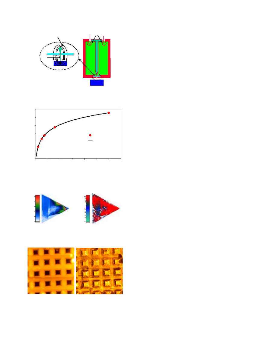
Accurate measurement of dielectric constant by theoretical
fitting of tip to the sample approaching curve.
Imaging:
Conductivity and Topographic: Q scanning and Topogra-
phy scanning at constant frequency mode
Dielectric Constant and Tangent Loss: f scanning and Q
scanning in constant force (soft-contact) mode or constant
height mode
Non-Linear Dielectric (Ferroelectric): Bias electrical field
can be applied for non-linear dielectric materials in f and Q
scanning
Applications
·
Dielectric constant and tangent loss
·
Conductivity/sheet resistance
·
Resistivity for semi-insulating GaAs wafers
·
Doping for Si semiconductor process control
·
Impedance continuity for defects analysis
·
High throughput screening of combinatorial libraries
·
Non-destructive evaluation applications
For more information, please contact:
Mr. Carson Huang,
MTI Corporation
532 Jacuzzi Street, Bldg. 3-H, Richmond, CA 94804,
Tel. 510-525-3070, Fax. 510-525-4728, E-mail
mti@mticrystal.com
Sample
Coupling Loops
Electrical Field
Sample
Microwave Resonator Probe
Tip
Sr
Ca
0.10
0.00
0.01
0.05
500
400
100
300
0
200
Sr
BBa
Ca
Sr
Ba
Ca
tan
0.10
0.00
0.01
0.05
0.10
0.00
0.01
0.05
500
400
100
300
0
200
500
400
100
300
0
200
Sr
Ca
MgO (9.5)
LAO (24)
Ceramic A (35)
Ceramic B (78)
STO (300)
0
10
20
30
40
50
60
0
50
100
150
200
250
300
350
Dielectric constant
Re
so
na
nt
f
r
e
q
u
e
nc
y
(M
H
z
)
Experimental
Fitting Curve
f
0
= 2785 MHz
A = 0.004969
MgO (9.5)
LAO (24)
Ceramic A (35)
Ceramic B (78)
STO (300)
0
10
20
30
40
50
60
0
50
100
150
200
250
300
350
Dielectric constant
Re
so
na
nt
f
r
e
q
u
e
nc
y
(M
H
z
)
Experimental
Fitting Curve
f
0
= 2785 MHz
A = 0.004969
EMP Topography Scan of surface (left) and Q
Scan of conductivity (right) of a standard metal
grid (Park Scientific Instruments) with 9.9
µ
m
square pattern, 0.2
µ
m thickness and 3.3
µ
m gaps.
